As technology advances at an astonishing rate, we find ourselves relying more and more on tiny components that make up our devices. One such component is the silicon wafer, the essential building block for modern microchips. Have you ever wondered how these silicon wafers can be so powerful yet so small?
The answer lies in their design, specifically when they are patterned for optimal performance. Patterned silicon wafers play a vital role in the development of next-gen microchips, enabling faster, more efficient devices that we use every day. Keep on reading.
Understanding Silicon and Its Importance
Silicon is a common element found in sand and rocks. Because of its unique properties, it has become the most widely used semiconductor material in electronics.
It can conduct electricity under certain conditions, making it perfect for use in circuits found in microchips. Microchips, in turn, are the tiny brains behind our devices, allowing them to process information and carry out functions.
Why is silicon so important? For starters, it’s abundant and relatively inexpensive compared to other materials. This helps manufacturers make many microchips for less money.
This is important because the demand for technology keeps rising. However, as we push the limits of what silicon can do, it’s vital to improve its capabilities, which is where patterned silicon wafers come in.
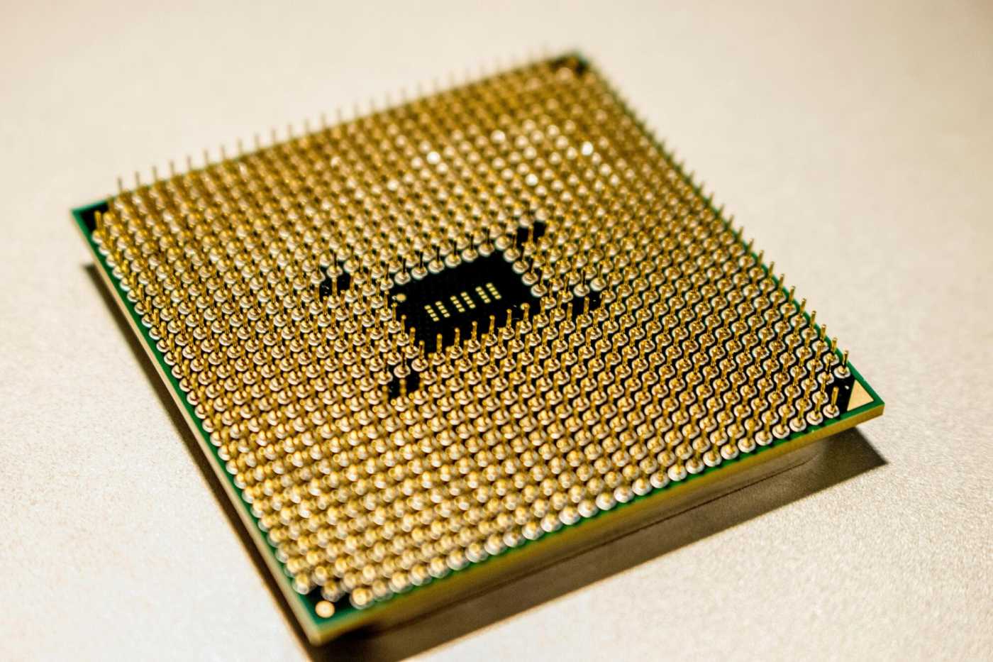
The Role of Patterned Silicon Wafers
Patterned silicon wafers are unique wafers with specific designs etched on their surfaces. These patterns allow for better conductivity and improved performance when creating microchips.
Think of it like a road map for electrical signals in a chip. The clearer and more organised the map, the faster and more efficiently signals can travel.
Using advanced techniques like photolithography, manufacturers can create intricate designs on silicon wafers. This process shines light through a mask with the desired pattern.
This lets the pattern transfer onto the silicon surface. The result? A finely tuned product that enhances microchip functionality.
Benefits of Patterned Silicon Wafers
There are several benefits of using patterned silicon wafers in microchip production. This includes:
Increased Efficiency
One major benefit is the increased efficiency of the microchips produced. The precise patterns etched on the wafers allow for better organisation of electrical pathways. This means that data can be processed more quickly, leading to faster devices.
Reduced Size
Patterning silicon wafers helps makers build smaller, more compact devices. They can do this without losing power or functionality. This is important now because portable technology, like smartphones and tablets, is very popular.
Improved Performance
Better-patterned wafers enhance the ability of microchips to handle multiple tasks simultaneously. This means devices can perform more complex operations efficiently and with greater speed. The result is improved processing power and overall system performance.
Higher Production Precision
Patterned silicon wafers improve the accuracy of microchip manufacturing. Advanced photolithography techniques make sure each circuit and pathway is placed with tiny precision. This reduces errors during production and enhances the overall reliability of the chips.
Scalability in Manufacturing
Using patterned wafers allows manufacturers to produce chips consistently at large scales. The repeatable nature of wafer patterning ensures uniform quality across batches. This scalability supports mass production while keeping costs and defects low.
How Patterned Silicon Wafers Are Made
Creating a patterned silicon wafer involves several steps, beginning with the raw silicon ingots. The ingots are sliced into thin wafers, usually just a fraction of a millimetre thick. After that, the wafers undergo a cleaning process to remove any impurities that could affect their performance.
Next comes the most critical step: the patterning process itself. Photolithography is employed to transfer designs onto the wafer.
After exposing the wafer to light, it undergoes a chemical development process that helps to reveal the pattern. Once the pattern is etched, additional layers of materials may be added to enhance the wafer’s properties further.
Future Innovations in Patterned Silicon Wafers
As technology continues to evolve, so does the development of patterned silicon wafers. Researchers and scientists are always looking for new patterns and materials. These could help create better microchips.
One exciting area of research focuses on creating 3D structures on silicon wafers. Manufacturers stack layers of circuits to create complex designs. This boosts chip performance beyond previous limits.
New materials like graphene or gallium nitride, used with silicon, could improve patterned silicon wafers. These materials have special electrical traits.
They could make microchips faster and more efficiently. Scientists are looking at ways to mix these advanced materials with silicon wafer technology. This could open up nearly limitless possibilities for the future.
The Impact of Patterned Silicon Wafers on Our Daily Lives
The benefits of patterned silicon wafers extend beyond the technology industry. These advancements have a direct impact on our daily lives.
Consider how smoothly our smartphones work, how fast computers process tasks, and how quickly video game consoles respond. All these devices rely on silicon wafers that have been expertly designed to maximise their potential.
Improved microchips make gadgets better. They also drive advancements in medicine, renewable energy, and artificial intelligence. Microchips in medical devices help doctors diagnose and treat patients better.
Also, chips in renewable energy make solar power more efficient. As innovative technologies become more prevalent, the role of patterned silicon wafers will only grow in importance.
The Challenges Ahead
Despite the significant advancements made with patterned silicon wafers, challenges remain. One of the biggest hurdles is the need for continuous innovation to keep up with increasing demands.
As devices become more capable, they require faster and more efficient chips. Manufacturers must always find ways to push the limits of silicon technology.
Another challenge is the environmental impact of silicon production. The process of creating silicon wafers can generate waste and consume energy. Scientists are exploring green manufacturing practices to minimise this impact, making the production of patterned silicon wafers more sustainable.
Patterned Silicon Wafers Enabling Next-Gen Microchips
Patterned silicon wafers are revolutionising the way we think about next-gen microchips and technology as a whole. Their incredible benefits have enabled significant advancements in various fields, leading to devices that improve our lives in countless ways.
As innovation continues to flourish, exploring new materials and designs will help us harness the full potential of silicon. By embracing these technologies, we set the stage for a smarter and more efficient future.